- 您现在的位置:买卖IC网 > Sheet目录1228 > MAX4273EVKIT (Maxim Integrated Products)EVAL KIT FOR MAX4273
�� �
�
�3V� to� 12V� Current-Limiting� Hot-Swap� Controllers�
�with� Autoretry,� DualSpeed/BiLevel� Fault� Protection�
�MOSFET� with� a� duty� cycle� equal� to� t� ON/� t� RETRY� and� with�
�a� current� equal� to� I� FAST,SET� .� Therefore,� particular� care�
�has� to� be� taken� when� choosing� between� immediate�
�retry� and� board� space� needed� to� manage� the� power�
�dissipation� capabilities� of� the� MOSFET� (see� Thermal�
�Considerations� ).� The� duty� cycle� is� fixed� to� 1/32� for� the�
�MAX4272,� but� can� be� varied� in� the� MAX4273� by� choos-�
�ing� CTIM� and� C� TON� independently.�
�Additional� External� Gate� Capacitance� (CEXT)�
�An� external� gate� capacitance� can� be� connected� at�
�GATE.� This� increases� the� time� required� to� enhance� the�
�MOSFET� and� further� limits� the� output� rise� time.� In� the�
�MAX4271/MAX4272,� connect� the� external� capacitor�
�between� GATE� and� GND.� In� the� MAX4273,� the� external�
�capacitor� can� be� connected� between� GATE� and� CEXT�
�or� GND.� If� the� capacitor� is� connected� to� CEXT,� it� is� dis-�
�charged� to� ground� during� a� slow� comparator� fault� but� it�
�is� left� floating� during� a� fast� comparator� fault;� this� allows�
�the� device� to� turn� off� the� external� MOSFET� faster� during�
�critical� faults.� (CEXT� is� biased� at� V� IN� ;� therefore,� use� a�
�nonpolarized� capacitor).� Capacitance� connected� from�
�GATE� to� CEXT� does� little� to� decrease� the� regulated� cur-�
�rent� ripple.� Add� a� small� capacitor� (5nF)� from� GATE� to�
�GND.� See� the� charging� and� discharging� time� vs.� C� GATE�
�graphs� in� the� Typical� Operating� Characteristics� .�
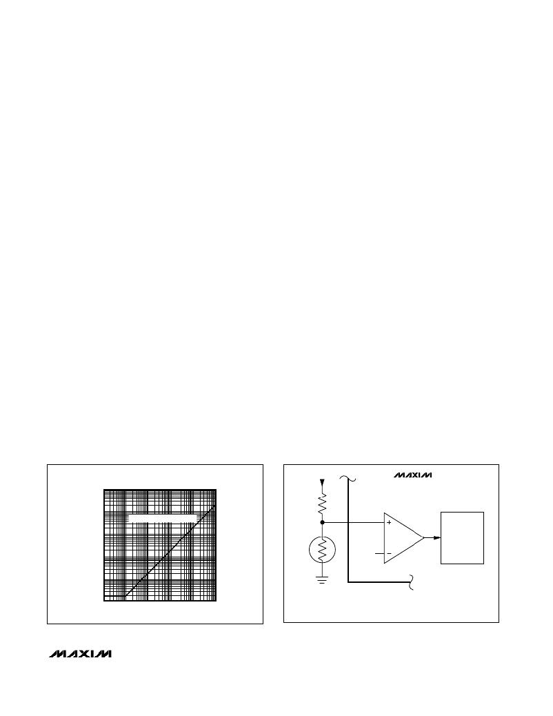
�Slow� Comparator� Response� Time� (CSPD)�
�The� slow� comparator� threshold� is� set� at� 50mV,� and� its�
�response� time� is� determined� by� the� external� capacitor�
�connected� to� CSPD� (Figure� 10).�
�A� minimum� response� time� of� 20μs� (typ)� is� achieved� by�
�leaving� this� pin� floating.� This� time� is� determined� inter-�
�nally� and� is� not� affected� by� stray� capacitance� at� CSPD�
�(up� to� 100pF).�
�SLOW� COMPARATOR�
�Set� the� slow� comparator� response� time� to� be� longer�
�than� the� normal� operation� load� transients� (see� Slow�
�Comparator� ).�
�ON� and� Reset� Comparators�
�The� ON� comparator� controls� the� ON/OFF� function� of�
�these� devices.� The� ON� comparator� is� a� precision� volt-�
�age� comparator� that� can� be� used� for� temperature� moni-�
�toring� or� as� an� additional� UVLO� (Figure� 11).� The�
�MAX4273� also� features� an� uncommitted� delayed� com-�
�parator.� This� comparator� can� be� used� for� voltage� moni-�
�toring,� power� sequencing,� or� for� generating� a� power-on�
�reset� signal� for� on-card� microprocessors� (Figure� 12).�
�Both� comparator� threshold� voltages� are� set� at� V� REF� /2� =�
�0.6V� with� a� 3mV� (typ)� hysteresis.�
�The� uncommitted� comparator� OUTC� output� is� an� open-�
�drain� output,� and� it� is� asserted� low� when� its� input� volt-�
�age� (INC)� is� below� the� threshold� voltage.� It� goes� into� a�
�high-impedance� state� 150ms� after� the� voltage� has� risen�
�above� the� threshold.� The� delay� for� negative-going�
�edges� is� 10μs.�
�Figure� 13� shows� the� MAX4273� used� to� monitor� precise-�
�ly� the� temperature� of� an� external� device� such� as� the�
�MOSFET.� This� configuration� uses� the� uncommitted�
�comparator� to� set� the� UVLO� at� a� higher� level� by� running�
�its� output� into� the� ON� comparator’s� input.�
�The� ON� comparator� initiates� startup� when� its� input� volt-�
�age� (V� ON� )� rises� above� the� threshold� voltage� and� turns�
�off� the� MOSFET� when� the� voltage� falls� below� the� thresh-�
�old.� The� propagation� delay� is� 10μs� going� high� or� low.�
�The� ON� comparator� is� also� used� to� reset� the�
�MAX4271/MAX4273� (when� CTIM� =� V� IN� )� after� a� fault�
�condition� (see� Latched/Autoretry� ).�
�V� REF�
�1000�
�100�
�10�
�RESPONSE� TIME� vs.� CSPD�
�t� CSPD� (ms) = 0.2 x CSPD (nF)�
�R1�
�ON�
�MAX4271�
�MAX4272�
�MAX4273�
�LOGIC�
�CONTROL�
�1�
�NTC�
�R2�
�0.6V�
�0.1�
�0.01�
�0.01�
�0.1�
�1� 10�
�CSPD� (nF)�
�100�
�1000�
�R1� =� R2� ?� (V� REF� /� O.6� -� 1)�
�R2� =� VALUE� OF� THE� NTC� RESISTOR� AT� THE� LIMIT� TEMPERATURE�
�V� REF� =� ANY� REFERENCE� VOLTAGE� AVAILABLE� OR� V� IN�
�Figure� 10.� Slow� Comparator� Response� Time� vs.� CSPD�
�Figure� 11.� Temperature� Monitoring� and� Protection�
�______________________________________________________________________________________�
�19�
�发布紧急采购,3分钟左右您将得到回复。
相关PDF资料
MAX4278EVKIT-SO
KIT EVALUATION FOR MAX4178,4278
MAX44265EVKIT#
KIT EVAL FOR 44265
MAX4754AEVKIT+
KIT EVAL FOR MAX4754
MAX4810EVKIT+
KIT EVAL FOR MAX4810
MAX4886EVKIT+
KIT EVAL FOR MAX4886
MAX4948EVKIT+
KIT EVAL FOR MAX4948
MAX4983EEVKIT+
KIT EVAL FOR MAX4983
MAX4989EVKIT+
EVALUATION KIT FOR MAX4989
相关代理商/技术参数
MAX4274ABESA
功能描述:运算放大器 - 运放 Integrated Circuits (ICs)
RoHS:否 制造商:STMicroelectronics 通道数量:4 共模抑制比(最小值):63 dB 输入补偿电压:1 mV 输入偏流(最大值):10 pA 工作电源电压:2.7 V to 5.5 V 安装风格:SMD/SMT 封装 / 箱体:QFN-16 转换速度:0.89 V/us 关闭:No 输出电流:55 mA 最大工作温度:+ 125 C 封装:Reel
MAX4274ABESA+T
功能描述:运算放大器 - 运放 RoHS:否 制造商:STMicroelectronics 通道数量:4 共模抑制比(最小值):63 dB 输入补偿电压:1 mV 输入偏流(最大值):10 pA 工作电源电压:2.7 V to 5.5 V 安装风格:SMD/SMT 封装 / 箱体:QFN-16 转换速度:0.89 V/us 关闭:No 输出电流:55 mA 最大工作温度:+ 125 C 封装:Reel
MAX4274ABESA-T
功能描述:运算放大器 - 运放
RoHS:否 制造商:STMicroelectronics 通道数量:4 共模抑制比(最小值):63 dB 输入补偿电压:1 mV 输入偏流(最大值):10 pA 工作电源电压:2.7 V to 5.5 V 安装风格:SMD/SMT 封装 / 箱体:QFN-16 转换速度:0.89 V/us 关闭:No 输出电流:55 mA 最大工作温度:+ 125 C 封装:Reel
MAX4274ABEUA
功能描述:运算放大器 - 运放 Integrated Circuits (ICs)
RoHS:否 制造商:STMicroelectronics 通道数量:4 共模抑制比(最小值):63 dB 输入补偿电压:1 mV 输入偏流(最大值):10 pA 工作电源电压:2.7 V to 5.5 V 安装风格:SMD/SMT 封装 / 箱体:QFN-16 转换速度:0.89 V/us 关闭:No 输出电流:55 mA 最大工作温度:+ 125 C 封装:Reel
MAX4274ABEUA-T
功能描述:运算放大器 - 运放
RoHS:否 制造商:STMicroelectronics 通道数量:4 共模抑制比(最小值):63 dB 输入补偿电压:1 mV 输入偏流(最大值):10 pA 工作电源电压:2.7 V to 5.5 V 安装风格:SMD/SMT 封装 / 箱体:QFN-16 转换速度:0.89 V/us 关闭:No 输出电流:55 mA 最大工作温度:+ 125 C 封装:Reel
MAX4274ACESA
功能描述:运算放大器 - 运放
RoHS:否 制造商:STMicroelectronics 通道数量:4 共模抑制比(最小值):63 dB 输入补偿电压:1 mV 输入偏流(最大值):10 pA 工作电源电压:2.7 V to 5.5 V 安装风格:SMD/SMT 封装 / 箱体:QFN-16 转换速度:0.89 V/us 关闭:No 输出电流:55 mA 最大工作温度:+ 125 C 封装:Reel
MAX4274ACESA-T
功能描述:运算放大器 - 运放
RoHS:否 制造商:STMicroelectronics 通道数量:4 共模抑制比(最小值):63 dB 输入补偿电压:1 mV 输入偏流(最大值):10 pA 工作电源电压:2.7 V to 5.5 V 安装风格:SMD/SMT 封装 / 箱体:QFN-16 转换速度:0.89 V/us 关闭:No 输出电流:55 mA 最大工作温度:+ 125 C 封装:Reel
MAX4274ACEUA
功能描述:运算放大器 - 运放
RoHS:否 制造商:STMicroelectronics 通道数量:4 共模抑制比(最小值):63 dB 输入补偿电压:1 mV 输入偏流(最大值):10 pA 工作电源电压:2.7 V to 5.5 V 安装风格:SMD/SMT 封装 / 箱体:QFN-16 转换速度:0.89 V/us 关闭:No 输出电流:55 mA 最大工作温度:+ 125 C 封装:Reel